6/5/10: NACSA 2010 Annual Conference – Emerging Technologies of the Next Decade

Events on May 11th, 2010 Comments Off on 6/5/10: NACSA 2010 Annual Conference – Emerging Technologies of the Next Decade

Presentation Materials:
1. 2010 NACSA Annual Conference Slides

2. NACSA Presidents’ Presentations

3. Presentation of Mr. Lip-Bu Tan

4. Presentation of Mr. Stan Myers

5. Presentation of Mr. Mario Morales

6. Zhenjiang City’s Presentation

Date: June 5, 2010

Time: 9:30AM-5:00PM

Location: Santa Clara Marriott, Hall of Cities Ballroom

Address: 2700 Mission College Boulevard, Santa Clara, CA‎ 95054
Google Map

You may using the parking lots nearby for free. If you want to use hotel’s parking lot, a discount will be applied (Please pay at the registration desk).

Cost: Conference: Free, Lunch: $25

In the coming decade, will the semiconductor industry continue the same growth as the past several decades following the direction of ‘Moore’s law’? How will cloud computing, xPU based personal computers and smart phones share the computation power? What is the role of solid state memories in the future high performance computation? ‘NACSA 2010 Annual Conference: Emerging Technologies of the Next Decade’ will help to answer all these questions you might have in mind.

NACSA 2010 Annual Conference will be held on June 5 at the Hall of Cities Ball Room, Santa Clara Marriott. We are greatly honored to have a group of distinguished speakers to share their perspectives and visions on emerging technologies in the coming decade.

Dr. Sehat Sutardja, Chairman, President and CEO of Marvell Technology Group will give a keynote speech titled “The Social Implications of Moore’s Law in this Decade”. Mr. Young Joon Choi, VP of Samsung Electronics, will be offering his speech titled “Future memory and storage technologies”.
Mr. Stan Myers, President and CEO of SEMI, will give a speech on “Emerging Technologies and Adjacent Markets” while Mr. Mario Morales, Program VP of IDC, will presenting “Reinventing Taiwai and China Inc. – What Is Next For Taiwan and China’s Semiconductor Industry?”. Being SVP of NVIDIA, Mr. Phil Carmack will be at a unique vantage to share his perspectives on the revolution of GPU. To round out this exciting event, Mr. Lip-bu Tan, Chair of Walden International and CEO of Cadence, will cover the Agile Strategies for Profit in the Global Economy.

Plated lunch will be served in the California Ball Room. We are honored to have Mr. Chuck Reed, the Mayer of San Jose, to be there to congratulate the event. A delegation from the city of Zhenjiang will be presenting “Zhenjiang in Silicon Valley – 2010” with the city’s attractive innovation programs. Those who are interested in starting business or establishing operations in China will have a chance of face-to-face interaction with the decision makers and are strongly encouraged to attend. Only $25 will be charged for the whole event as NACSA will partially cover the cost of your lunch.

Spaces for the conference and the lunch event are limited, please follow the links above to register.

For more information on NACSA and its activities, please refer to our website www.nacsa.com.

Agenda
Location: Hall of Cities Ballroom, Santa Clara Marriott, 2700 Mission College Boulevard, Santa Clara, CA 95054
Time: 9:30am-5:00pm, June 5, 2001 (Saturday)

Morning Session
9:30-10:00am Registration and Social
10:00-10:30am Welcoming Speech
Larry Ge & Renxin Xia, NACSA Presidents
10:30-11:15am “The Social Implications of Moore’s Law in this Decade”
Sehat Sutardja, PhD., Chairman, President and CEO, Marvell Technology Group, Ltd.
11:15-12:00pm “Reinventing Taiwan and China Inc.- What Is Next For Taiwan and China’s Semiconductor Industry?”
Mario Morales, Program VP, Semiconductors & EMS, IDC
12:00-12:15pm “Innovative Cities in China-the Trend for the Next Decade”
City of Zhenjiang

Luncheon in California Ballroom
12:15-1:30pm “Zhenjiang in Silicon Valley – 2010”
Sponsored by City of Zhenjiang

Afternoon Session
1:30-2:15pm “Emerging Technologies and Adjacent Markets”
Stan Myers, President & CEO, SEMI
2:15-3:00pm “A Revolution in Mobile Computing”
Phil Carmack, SVP, NVIDIA
3:00-3:15pm Break / NACSA Board Member Election
3:15-4:00pm “Future Memory and Storage Technologies”
Young Joon Choi, VP, Future Product Planning, Samsung Electronics Corporation
4:00-4:45pm “Innovating Profitably in the Next Decade”
Lip-bu Tan, Chair, Walden International & CEO, Cadence
4:45-5:00pm Concluding Remarks / Board Member Election Results

Speakers’ Bio


Sehat Sutardja, PhD.
Chairman, President & CEO, Marvell Technology Group, Ltd.

Dr. Sutardja is the Chairman, President and Chief Executive Officer of Marvell Technology Group, Ltd. He is widely regarded as one of the pioneers of the modern semiconductor age. His breakthrough designs and guiding vision have revolutionized numerous industry segments, from data storage to the high performance, low power chips now driving the growing global markets for mobile computing and telephony. His lifetime passion for electronics began early; he became a certified radio repair technician at age 13 and has been designing components and systems ever since. For his relentless innovation, he has been awarded more than 150 patents and has been named a Fellow of IEEE. In 2006, Dr. Sutardja was recognized as the Inventor of the Year by the Silicon Valley Intellectual Property Law Association.

As co-founder of Marvell Technology Group Ltd., Dr. Sutardja has served as President, Chief Executive Officer and Co-Chairman of its Board of Directors since its inception and as Chairman of the Board since 2003. In addition, he serves as President, Chief Executive Officer, and as a Director of Marvell’s U.S. operating subsidiary, Marvell Semiconductor, Inc. While remaining deeply involved in the daily challenges of running a global growth company, Dr. Sutardja participates heavily in Marvell’s engineering and marketing efforts across analog, video processor, and microprocessor design while offering input across all of the company’s other product lines.
Dr. Sutardja has become an internationally-recognized proponent of new energy efficiency standards for consumer electronics. To that end, he has been working with the governments in both the US and China to establish efficiency performance standards that could produce significant cost and carbon savings.

Dr. Sutardja holds Master of Science and PhD degrees in Electrical Engineering and Computer Science from the University of California at Berkeley. He received a Bachelor of Science degree in Electrical Engineering from Iowa State University.
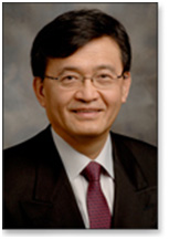
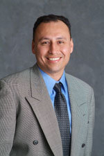

Lip-Bu Tan
President & CEO, Cadence Design Systems, Inc.
Chair, Walden International

Lip-Bu Tan is President and Chief Executive Officer of Cadence Design Systems, Inc. He has been a member of the Cadence Board of Directors since 2004 and serves as a member of the Finance and Technology Committees of the Board. He also serves as chairman of Walden International, a venture capital firm he founded in 1987. Prior to founding Walden, Tan was Vice President at Chappell & Co. and held management positions at EDS Nuclear and ECHO Energy.

Tan received an M.S. in nuclear engineering from the Massachusetts Institute of Technology, an MBA from the University of San Francisco, and a B.S. from Nanyang University in Singapore. He serves on the Board of Directors of Flextronics, SINA, and SMIC. He is also a board member of the Electronic Design Automation Consortium (EDAC) and the Global Semiconductor Alliance (GSA).
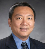

Philip J. Carmack
Sr. VP, Mobile Business Unit, NVidia

Phil Carmack has served as senior vice president of NVIDIA’s mobile business unit since 2008 Prior to joining the company in 2000, he was executive vice president of research and development at 3dfx Interactive; senior vice president and chief operating officer at Gigapixel; and was chief executive officer and founder of Raydiant, a graphics silicon technology company.


Youngjoon Choi
Vice President, Memory System Solution Group, Memory Division,
Semiconductor Business, Samsung Electronics

Throughout his career with Samsung Electronics for over 25 years, he has led the development of advanced memory technologies through product engineering, product designing, and flash product planning. He joined Samsung Electronics in 1985 and had worked on design and device engineering of non-volatile memory, especially on NAND Flash. In 1998, he moved to technical marketing to bring up NAND applications which was only sprouting then. He led the development of Flash solution products in Samsung while working with industry partners to enable NAND Flash infrastructure in controllers and system software. He is currently leading memory system solution group in Samsung, responsible for creating memory subsystem solutions and future memory architectures.


Mario Morales
Program Vice President, Semiconductors and EMS
IDC

Mario Morales is the vice president of IDC’s Semiconductors research program. He is responsible for in-depth analysis, evaluation of emerging markets, forecasting, and research of major semiconductor application areas such as embedded devices and microprocessors, wireless, personal computing, wired communications, and consumer.

Mr. Morales is an industry analyst with extensive experience in managing a multinational research team of analysts, management consultants, and business development managers. Key strengths include international business development and driving strategic relationships with semiconductor and Information Communications and Technology (ICT) vendors. Strong knowledge of IT industry, with a specialization in semiconductors, embedded devices, memory, and wireless. Over 19 years of semiconductor expertise, including management consulting, market assessment, valuation of leading companies, creation of industry leading market models, and competitive analysis. Responsible for initiating IDC’s coverage of the semiconductor and EMS market segments including building a successful and strategic business franchise for IDC. Strong network in the semiconductor industry and Asia Pacific region; trusted advisor to leading executives and financial community on market direction, targeting strategic customers, market segmentation, product positioning, competition, M&A due diligence, and platform branding. His career includes past positions with NEC Electronics and Dataquest.

Mr. Morales earned a B.S. degree in business administration (finance) at San Jose State University.
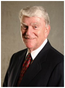
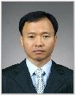

Stanley T. Myers
President and Chief Executive Officer, SEMI

Stanley T. Myers is the President and CEO of SEMI. Headquartered in San Jose, California, SEMI is a global industry association serving companies that provide equipment, materials and services used to manufacture semiconductors, displays, nano-scaled structures, micro-electromechanical systems (MEMS) and related technologies.

Prior to his appointment as SEMI president in 1996, Myers worked for 17 years at Siltec Silicon, a manufacturer of silicon wafers, based in Salem, Oregon. He served as president and CEO since 1985, and in 1986 he completed negotiations for the acquisition of Siltec by Mitsubishi Materials Corporation. In July 1996, Siltec officially changed its name to Mitsubishi Silicon America Corporation. Prior to Siltec, Myers worked for Monsanto Corporation for 18 years.

Myers continues to serve on the SEMI board of directors, a post to which he was elected in 1988. He sits on the boards of Ecosol, SKW Corporation, NCT Corp. and MATEC (Maricopa Advanced Technology Education Center). Myers also is a member of the Engineering Advisory Board to the School of Engineering, San Jose State University.

Myers earned a bachelor’s degree in chemical engineering from the University of Kansas.>

NACSA and Zhang Jiang to Build “North America Innovation Center” in Shanghai

Events on March 9th, 2010 Comments Off on NACSA and Zhang Jiang to Build “North America Innovation Center” in Shanghai

NACSA and Zhang Jiang to Build “North America Innovation Center” in Shanghai, Returnees Are Welcome to Join

NACSA和张江集团将在上海携手创立”北美创新中心”
欢迎在上海的前会员和高科技领域海归和专业人士参加

秉承北美中国半导体协会 North America Chinese Semiconductor Association (NACSA) 的一贯宗旨-为广大会员服务,作中美科技、文化交流的桥梁,也为了近年来在中国经济迅猛发展的背景下已经或有志回国在上海投资、创业、创新的企业家、高科技、专业人士和企业提供更好的服务,促进上海和北美两地以及已经回到上海创业、工作的广大会员和高科技、专业人士间的更广泛深入的交流与合作,推动张江作为中国高科技高地与硅谷地区更好地对接,经过NACSA和张江高科技园区初步协商,决定共同在上海张江创办北美创新中心。

张江作为中国高科技产业高地,已形成了以集成电路、软件、生物医药等产业为基础的高科技产业集群。作为当前国内最具规模的高科技园区之一,张江一直致力予鼓励自主创新,打造良好的创业环境。

创新中心的宗旨就是要利用这样一个多功能平台, 背靠张江集团在上海的地理和资源优势和NACSA在北美特别是硅谷高科技各行业的广泛联系和影响力,更好地为在上海的会员提供更多更好的服务和交流的机会,共创多赢。

创新中心的场地初步落实在风景优美、交通方便的、高科技行业最集中的上海张江孵化器园区,NACSA和张江将配备专人负责,定期举办有关创新、创新、企业成长方面的专题讲座,讨论会, 以及联谊活动。中心还将设立专门网站(页),定期公布相关信息, 以及虚拟孵化器。会员和活动将涉及半导体行业,新能源,生物医药,IT等各高科技行业领域。

热烈欢迎回到上海地区的NACSA前会员,和从各国回到上海投资、创业,和工作的企业家,高科技和专业人士加入。敬请网上注册RSVP。北美创新中心会员也将自动成为NACSA Shanghai Chapter会员。

网上注册RSVP

>

Honeywell Specialty Materials Position

Job Listing on March 9th, 2010 Comments Off on Honeywell Specialty Materials Position

This position is located in Shanghai ,

Zhangjiang High Tech Park .

Pay is competitive.

Contact: Song.Xue@Honeywell.com if interested.

Honeywell Specialty Materials Position Specification

Position: Senior Tech Manager
Location: Shanghai , China
Reports to: Technology Director

Band: 4
Specific Responsibilities

Managing Electronic Polymer and Thermal Interface Material Group

· Lead R&D team to develop state of the products for electronics polymer and thermal interface material and to provide application support for customers.

· Partner with customers to better understand current and future electronic material technology needs and requirements.

· Lead technical efforts to support Sales & Marketing team to develop new customers and expand business in electronic materials in Asia Pacific.

· Develop technology pipeline/platforms in electronic materials and align project scope with global business strategy.

· Build strong EM application capabilities and strengthen bonding with cross-functional teams.

· Keep effective communication with various levels of organization on project status/team status and more.

· Maintain good documentation and keep IP well protected. IP Portfolio management.

· Build and develop HEM team including hiring, coaching, mentoring team members; influence other members of matrix organization for leadership leverage to achieve business vision.
Position Scope

Managing Electronic Polymer and Thermal Interface Material group, including management on budget/lab/people/R&D portfolio; customer interface, roadmap development.
Reporting Relationship

This position will report to Technology Director
Educational & Other Requirements

§ PH.D in composite or polymer science and engineering disciplines with min 5 years industrial experiences; or Master degree with min 7 years industrial experiences

§ Solid experiences in electronic polymer, thermal interface materials and in new product introduction

§ Ability to work in a matrix environment.

§ Customer focus and results oriented

§ Excellent leadership and teamwork skills.

§ Excellent written and oral English communication skills.

§ Ability to work and influence peers and upper management.

§ Good project management skills and ability to handle varied priorities and exceed expectations>

Seminar Summary of "High-tech Seminar Series: Industry Landscape in Mobile Computing"

Events on March 1st, 2010 Comments Off on Seminar Summary of "High-tech Seminar Series: Industry Landscape in Mobile Computing"

With more and more attention being focused on mobile computing, NACSA held a seminar to help our member understand the current two major platforms for mobile computing: ARM and x86 and their development trend. The theme is ‘Industry Landscape in Mobile Computing”. Two distinguished guest speakers, who are experts in the respective fields, shared their knowledge and perspectives on the challenges and market opportunities of mobile computing.

The 1st presentation was given by Dr. James Cheng, Director of Sales and Marketing in ST-Ericsson America. The title is ‘Industry landscape in mobile computing’. He provided details of mobile access technology, smartphone design challengers and his vision on mobile platforms. The next speaker was Mr. Anthony Yung, Marketing Manager of Intel Corp. The title of his speech is ‘Enabling the Mobile Internet’. He vividly demonstrated how the mobile computer will change people’s life.

The presentations were well received by NACSA’s members as well as outside attendees. We have to close the RSVP 4 days before the event keep the audience under the room capacity limit. Despite the raining weather, about 60 people attended the seminar. They showed a great deal of interest in the presented topics and asked so many questions that some of them had to be stopped to keep the time.

Presentations:
James Cheng, Industry landscape in mobile computing
Click here to download the presentation file (PDF format).

Anthony Yung, Enabling the Mobile Internet
Click here to download the presentation file (PDF format).

Photos of this event can be found:
http://picasaweb.google.com/NACSA.Gallery/02212009#

Leading Talent Program of the Suzhou Industrial Park (SIP)

Events on February 17th, 2010 Comments Off on Leading Talent Program of the Suzhou Industrial Park (SIP)

苏州工业园区第四届园区领军人才创业工程已开放网上申报

苏州工业园区第四届园区领军人才创业工程已开放网上申报,申报流程如下,所有申报项目须于2010年3月31日前完成网上申报。

1、网上申报须使用IE浏览器,并将http://tech.sipac.gov.cn 加入可信站点;

2、申报前先进行用户注册,用户密码将以电邮或手机短信(苏州本地)形式发送;

3、成功登陆后请至左侧项目申报栏目中选择领军人才项目开始网上申报;

4、网上申报时除基础信息栏须在表格内填写外,其他栏目可将word版申报书相关内容(包括图片)直接粘贴入表格;

5、申报结束请将word版申报书及相关附件材料上传至项目附件;

6、网上申报信息在初审结束前( 3月31日)可进行修改。


Suzhou Industrial Park (SIP) is launching a new round of application for Leading Talent Program (第四届科技领军人才创业工程) for the year 2010, interested companies please fill the form “苏州工业园区科技领军人才创业计划书(第4届)” and email to SIP contact lwei@sipac.gov.cn and NACSA contact ming_zhang@nacsa.com.

Application deadline: March 31, 2010.

Send your application to: lwei@sipac.gov.cn and ming_zhang@nacsa.com

咨询电话:苏州工业园区中小企业服务中心 011-86-512-67068010

苏州工业园区科技发展局 011-86-512-66680922

Please see following files for more details:

SIP is the platinum sponsor of NACSA.
>

2/27: NACSA Proudly Co-hosts: Wuxi in Silicon Valley 2010

Events on February 17th, 2010 Comments Off on 2/27: NACSA Proudly Co-hosts: Wuxi in Silicon Valley 2010

Happy New Year and may the year of the Tiger bring you health and prosperity!

The city of Wuxi is well known for its rich cultural heritage and mystic natural beauty. Additionally, the city has been booming in high-tech activities in the areas of solar energy, semiconductor IC, and IT. To strengthen its tie with Silicon Valley, a Wuxi delegation, led by top leaders of Wuxi’s New District, will visit Silicon Valley soon to have direct dialogs and information exchanges with business leaders, entrepreneurs, and professionals in the relevant fields in the Bay Area.

NACSA cordially invites members and friends, especially those who are interested in the following, to come and join us in the event:

  • Starting up business in China, especially in Wuxi/Yangzi River Delta area
  • Learning more about Wuxi’s 530 Project, its policy, procedure, and relevant successful stories
  • Learning more about China’s “Thousand-People” project and the strong support from Wuxi
  • Learning more about Wuxi’s ambition in investing in the next “big deal” in key technological areas including sensors, sensor network, etc.
  • Networking with high-ranking officials from Wuxi and other business leaders, entrepreneurs , professionals from the Bay Area like yourself.

Place: Crowne Plaza Hotel, 282 Almaden Blvd., San Jose, CA 95113
Google Map

Date & Time: February 27, 2010 (4:30 – 8:00pm)

主办: 无锡国家高新技术产业开发区管理委员会

协办: 北美半导体协会

主持: 阙尧尧

Agenda:

  • 16:30-17:00 注册、交流
  • 17:00-17:15 领导欢迎辞
  • 17:30-17:50 “感知中国”中心暨无锡新区传感网产业情况介绍
  • 17:50-18:10 无锡“千人计划”暨无锡新区归国创业人才创新创业专题汇报
  • 18:10-18:30 无锡“530计划”创业代表发言
  • 18:30-18:40 海外引才工作站授牌仪式
  • 18:40-19:00 Q&A互动
  • 19:00-20:00 招待晚宴

Registration:

Free on-line registration, seating is limited (up to 35).

RSVP is closed. Full capacity has been reached.

Agenda:

  1. 出席人员介绍
  2. 新区管委会主任嵇克俭: 无锡新区产业经济发展概况
  3. 太科园管委会 副主任张晓松: 无锡新区传感网产业规划及政策介绍
  4. 新区科技局副局长,530办常务副主任李敏云: 无锡新区“530”海归人员创业介绍暨无锡千人计划信息发布
  5. 530创业代表发言
  6. 现场交流互动及创业咨询

Delegation Members:

  • 嵇克俭 无锡国家高新技术产业开发区管理委员会 主任
  • 张晓松 无锡新区太湖国际科技园管理委员会 副主任
  • 袁泳娟 无锡新区经济发展局 副局长
  • 李敏云 无锡新区科技局 副局长
  • 郁江 无锡新区出口加工区管理局 副局长
  • 蒋帅 无锡新区信息产业科技园管理中心 副主任
  • 马奇明 无锡高新技术创业发展有限公司 副总经理
  • 阙尧尧 无锡软件服务外包园管理中心 副主任
  • 刘平 无锡高新技术创业服务中心招商部 部长
  • 潘子慧 无锡新区信息产业科技园管理中心招商部 项目经理

>

2/21/2010: NACSA proudly presents: "High-tech Seminar Series: Industry Landscape in Mobile Computing"

Events on February 6th, 2010 Comments Off on 2/21/2010: NACSA proudly presents: "High-tech Seminar Series: Industry Landscape in Mobile Computing"

Thanks to rapid advances in wireless technology, smartphones have brought ubiquity of internet accesses to the mass users. Though highly mobile and comparable in performance with netbooks, smartphones are not yet powerful enough as general purpose computing platforms. However, the convergence of computing and mobility is no longer a question of if, but one of when and in what form. The iPAD recently announced by Apple serves as a testimony to this trend. The convergence also means a massive market opportunity for the semiconductor industry.

To provide good user experience, the processors used in mobile computing platforms must have a decent performance for general purpose computing and multimedia playback and a low power consumption profile for long battery life per charge. Increasingly, these processors will also need to have on-die support for 3D graphics capability for gaming and possibly 3D contents.

NACSA cordially invite you to the first of our high-tech seminar series “Industry Landscape in Mobile Computing”, focusing on the two major platforms for mobile computing: ARM and x86. Two distinguished guest speakers, who are experts in the respective fields, will be sharing their knowledge and perspectives on these platforms as well as identifying the challenges and market opportunities facing them.

Time/Date: 1:00-4:00pm Sunday, Feb 21, 2010
Place: 47655 Warm Springs Blvd., Fremont, CA 94539

View Larger Map

Cost: Free
RSVP: RSVP has been closed due to limited seating.

Speakers Biographies

Anthony Yung, M.B.A., Marketing Manager, Intel Corp.

Topic: Enabling the Mobile Internet

Anthony Yung is Group Manager of Product Marketing at Intel's Ultra Mobile Group, whose charter is to build a vibrant business in the next generation handheld market segment. Prior to his current role, Mr. Yung held a variety of positions at Intel, including platform marketing of Centrino® mobile technology, product management of mobile Pentium®チIII processors, channel marketing, and long range planning. Prior to Intel, Mr. Yung was an analyst at Gartner Group / Dataquest and a design engineer at Sun Microsystems. Mr. Yung earned a bachelor's degree in electrical engineering and computer science from the University of California, Berkeley and an MBA from The Wharton School, University of Pennsylvania.

James Cheng, Ph.D., M.B.A., Director of Sales and Marketing, ST-Ericsson America

Topic: Industry Landscape in mobile computing, smart phone and tablet PC

James Cheng is Sales and Marketing Director for ST-Ericsson America in Santa Clara, CA responsible for key accounts including Microsoft, Intel, and Sierra Wireless in Western North America. Prior to ST-Ericsson, Mr. Cheng was Regional Marketing Director for Business Unit Mobile & Personal in America for NXP Semiconductors in San Jose, CA. He is responsible NXP solutions and application support for Nexperia cellular and connected entertainment (e.g., FM radio, GPS, media processor, Bluetooth, etc.) marketing in the region. Mr. Cheng has been in the wireless industry in the US for more than 15 years with responsibility ranging from system architecture development, technical management, product management, and early stage venture investing. Mr. Cheng holds a PhD in Electrical Engineering from Stony Brook University and an MBA from Stern School of Business of New York University.

Agenda
1-1:30 Registration
1:30-2:30 James Cheng’s talk
2:30-2:45 Q&A
2:45-3:45 Anthony Yung’s talk
3:45-4:00 Q&A

About NACSA

Founded in 1996 in the Silicon Valley, North America Chinese Semiconductor Association (NACSA) is a professional organization dedicated to the advancement of exchange and collaboration among Chinese professionals in semiconductor and related high-tech industries.

Riding the tide of globalization, the community of Chinese engineers and entrepreneurs in Silicon Valley and China has enjoyed a tremendous growth in recent years. Through event hosting, networking, and information sharing, NACSA has been instrumental in helping build a vibrant high-tech professional community serving the needs of these professionals. NACSA, with its 4000 strong members, is currently one of the largest and most active Chinese professional organizations in the US. NACSA members come from diverse fields in semiconductor and other high-tech related industries, including makers of optional devices, semiconductor chips, and PCs; system manufacturers; equipment manufacturers; design house; software; etc.

Committed to sharing information and resources and serving as a bridge between the US and China high-tech communities, NACSA’s mission is to strengthen networking among professionals, foster entrepreneurship in ethnic Chinese, and promote the exchange in the semiconductor and related high-tech industries. At NACSA, we believe in learning by doing and contributing before receiving.

Past NACSA seminar speakers include prominent CEOs, senior executives, and entrepreneurs from such well-known companies as Intel, Applied Materials, Cadence, MIPS Technology, Spreadtrum, UMC, TSMC, Go2Silicon, ViMicro, Broadcom Inc., Cypress Semiconductor, Keysi International, SH Zhangjiang, HK Science & Technology Parks, Goldman Sachs, and many others. NACSA seminars are well received and well attended with an average audience size of 300. Besides seminars and discussion forums, NACSA also hosts Spring/Summer picnic and forms special task teams. Each year, NACSA organizes delegations to China and hosts meetings with visiting high-tech delegations from China.

This seminar is cordially sponsored by Northwestern Polytechnic University, School of Global Education

ENN Group Is Hiring in the U.S.

Job Listing on September 23rd, 2009 Comments Off on ENN Group Is Hiring in the U.S.

Founded in 1989, ENN Group has grown to one of the largest renewable energy companies in China. Taking on clean energy innovation as its mission, ENN is committed to the production and application of clean energy. ENN Group has established CO2 recycling business as its core strategy and completed a clean energy value chain covering energy production, conversion, storage & transportation, and distribution & application. Our business ranges from coal-based clean energy, solar energy, to biomass-based energy, etc. Currently, ENN has more than 100 subsidiaries in over 80 cities across China and overseas and has more than 24000 employees with total asset of USD 4 billion.

ENN offers competitive compensation package. Interested candidates may E-mail their resume, cover letter and salary requirement for immediate consideration to: ennsolar_hr@enn.cn

Job ID: SE0901
Process Engineer

Description:
This position is responsible for process development and optimization for photovoltaic devices. Job location is Silicon Valley

Responsibilities:
– New technology development including hardware, process, and integration;
– Design and execute experiments for process development and improvement;
– Perform materials and device characterization;
– Conduct patent literature survey, IP filings, and other related IP protection activities;
– Oversee technical assistant for device fabrication and testing, equipment maintenance, chemical handling and waste disposal;
– Develop proposals for internal and external funding opportunities;
– Joint development work with major universities and research laboratories.

Qualifications:
– Advanced degree in Materials Science, Electrical Engineering, Physics, Chemical Engineering, or related technical disciplines;
– 1+ years industrial experience in thin film deposition (PECVD, PVD, Evaporator, etc.) and characterization;
– Extensive experience in solar cell fabrication and testing, solid understanding of device physics and modeling;
– Strong analytical skills and computer literacy;
– Understanding and experience with DOE and SPC;
– Strong oral and written communication skills including presentation skills;
– Strong problem-solving and trouble-shooting skills;
– Ability to make sound technical decisions and work independently, as well as in a team environment;
– Ability to acquire skills necessary for equipment maintenance and troubleshooting;
– Fluent speaking and writing in Mandarin highly preferred.

Job ID: SE0902
Materials Scientist

Description:
This position is responsible for materials research and device development for advanced solar energy technologies. Job location is Silicon Valley

Responsibilities:
– Conduct research and development of new materials for photovoltaic devices and technologies;
– Design and execute experiments for medium and long-term process development and improvement;
– Conceive and implement new technologies, products, and analytical methodologies and instrumentation;
– Develop long term plans, conceptual designs, and technology roadmaps;
– Perform materials and device characterization;
– Develop proposals for internal and external funding opportunities;
– Joint development work with major universities and research laboratories.

Qualifications:
– MS or Ph. D degree in Materials Science, Physics, Chemical Engineering, Electrical Engineering, or related technical disciplines;
– Broad knowledge and 5+ years hands-on work experience in at least one of the areas including: novel photovoltaic materials and devices; semiconductor or photovoltaic device physics and modeling; advanced thin film deposition and characterization, and related materials research, etc.;
– Extensive hands-on experience in metrologies and instrumentation for materials characterization and device testing;
– Strong analytical skills and computer literacy;
– Programming or data acquisition skills a plus;
– Strong oral and written communication skills including presentation skills;
– Strong problem-solving and trouble-shooting skills;
– Ability to make sound technical decisions and work independently, as well as in a team environment;
– Fluent speaking and writing in Mandarin highly preferred.

Job ID: SE0903
Sr. Process Technician

Description:
This position is responsible for supporting process development and lab maintenance. Job location is Silicon Valley

Responsibilities:
– Assist with and participate in process engineering projects;
– Perform start-up and daily operation of lab equipment and instruments;
– Record process conditions, experiment observations, and experimental data;
– Verify and approve equipment performance and plan uptime improvement;
– Generate and implement PM procedures, spare parts requests, purchase requisitions, etc.;
– Identify, troubleshoot, and correct equipment issues;
– Plan and execute a wide range of other support activities as required;
– Require attentiveness to safety precautions at all times;
– Comply with company safety policies and develop initiative in creating a safe working environment.

Qualifications:
– Bachelor or associate degree in science or engineering disciplines;
– 8+ years process and hardware support experience in semiconductor or solar industry;
– Demonstrated skills and capabilities to operate, diagnose, and repair a wide variety of semiconductor/solar equipment and tools;
– Experience in handling chemicals and gases commonly used for semiconductor or PV processing;
– Strong oral and written communication skills;
– Working knowledge of SPC and computer literacy;
– Flexibility to work on shifts/overtime/stand-by/on-call/holidays when required;
– Proficiency in Mandarin a plus.

中关村留学创业电子杂志

Partners Events on September 23rd, 2009 Comments Off on 中关村留学创业电子杂志


中关村留学创业电子杂志


2009
9

9/25: SVCW 2009 — Mobile AlwaysOn

Events on September 12th, 2009 Comments Off on 9/25: SVCW 2009 — Mobile AlwaysOn

The Silicon Valley-China Wireless Conference is the largest event to bring Silicon Valley and China together on wireless technologies, market trend and business opportunities. Because of excellent programs and high-profiled speakers, it attracts quality attendees and creates a unique opportunity for networking, product marketing and talent recruiting. We invite you to join other industry professionals together at SVCW2009 — Mobile AlwaysOn.

2:00PM – 6:00PM, Sept. 25, 2009 & 8:30AM – 7:00PM, Sept. 26, 2009. Computer History Museum, Mountain View, California

Register Today with Early Bird Special

For more information, please visit http://www.svcwireless.org